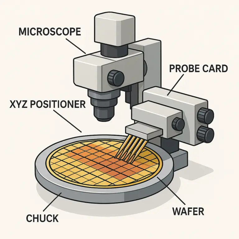
Advanced semiconductors’ relentless pursuit of higher density, greater speed, and lower power consumption has challenged the limits of traditional probe pin materials. Conventional metal alloys and plated tungsten pins struggle to maintain signal integrity and mechanical reliability during the millions of contact cycles required for modern \text{IC} and wafer testing. The solution lies in a material engineered for extremes: SiC Electrically Conductive Ceramics.
Our advanced SiC material, featuring an ultra-low electrical resistivity of 10^{-7} \Omega \cdot m, offers a paradigm shift for Wafer Test Probe Pins. This technology eliminates the historical trade-off between hardness (for longevity) and conductivity (for performance), providing the high-speed, high-purity, and extreme durability essential for next-generation chip validation.
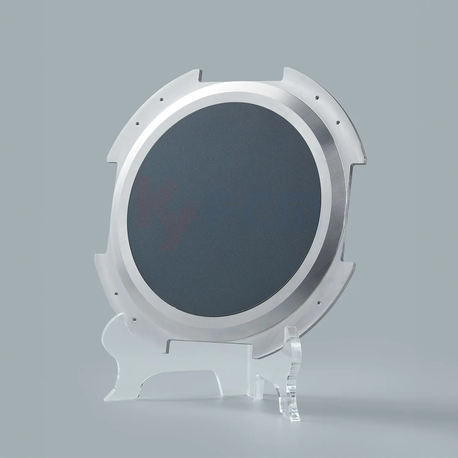
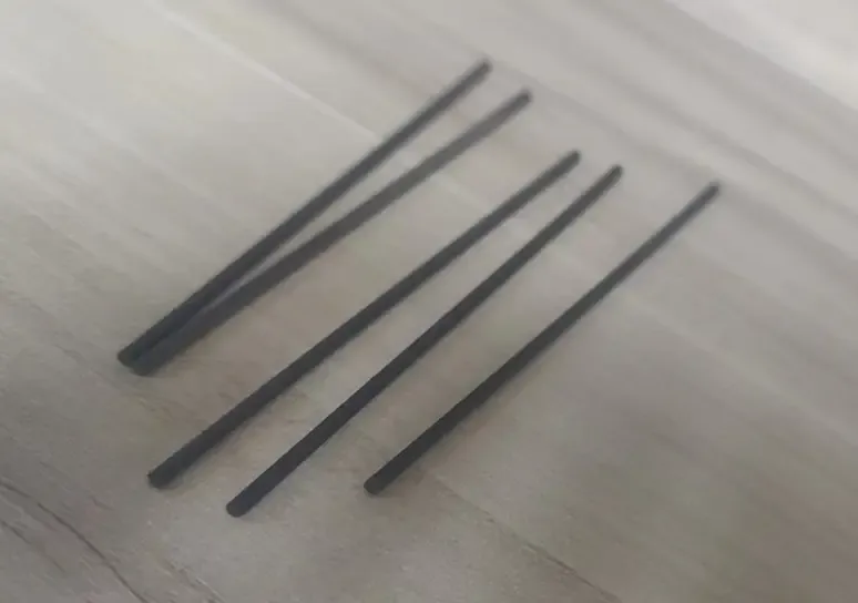 The SiC Conductive Ceramic Probe Pin
Section 1: The SiC Composite Advantage in Probe Pin Design
The superiority of our SiC conductive ceramic stems from its ability to integrate three previously separate functions into one homogeneous material:
| Property | Value | Direct Benefit for Probe Pins |
|---|---|---|
| Electrical Resistivity | 10^{-7} \Omega \cdot m | Guarantees minimal \text{RC} delay and signal distortion during \text{GHz}-speed testing. |
| Mechanical Hardness | 20.4 \pm 0.6 \text{GPa} | Ensures extreme wear resistance, dramatically increasing the operational lifespan of the probe pin. |
| Thermal Stability | High Conductivity & $1400^\circ C· Tolerance | Efficiently manages heat from large currents, preventing performance drift and thermal damage. |
| Surface Purity | Body-Conductive, Plating-Free | Eliminates particulate contamination risk and ensures stable contact resistance over time. |
Section 2: Solving the Three Critical Challenges in Chip Probing
Our ultra-low resistivity SiC conductive ceramics directly address the most expensive and time-consuming failures in wafer and chip testing:
1. Signal Integrity and \text{RC} Delay Elimination
Modern chips operate at increasingly high frequencies. Any resistance (R) within the probe pin creates an \text{RC} delay, which leads to signal degradation, inaccurate timing measurements, and compromised signal integrity.
- The Problem: Traditional metal probes, even with plating, contribute measurable resistance that distorts high-speed signals.
- The SiC Solution: The 10^{-7} \Omega \cdot m resistivity minimizes parasitic resistance along the signal path, ensuring that the probe functions as a near-perfect conductor. This is non-negotiable for reliably testing the timing, clock speed, and functional performance of high-frequency \text{IC}s.
2. Stable Voltage Delivery and \text{IR} Drop Mitigation
In testing high-power \text{CPUs}, \text{GPUs}, or power management \text{ICs}, the probe pins must safely deliver significant current without voltage loss.
- The Problem: Probe resistance causes significant voltage loss (\text{IR} drop) and generates heat (I^2 R). This means the \text{IC} under test receives less voltage than intended, leading to false test results and potential thermal instability.
- The SiC Solution: By dramatically lowering R via the 10^{-7} \Omega \cdot m material, the \text{IR} drop is virtually eliminated. This ensures that the voltage applied to the chip is precise and stable, maximizing the reliability and accuracy of power and functional testing. Furthermore, SiC’s high thermal conductivity rapidly dissipates the minimal heat generated.
3. Maximizing Lifespan and Eliminating Contamination
Test consumables are a major operating cost in semiconductor manufacturing, and probe tip contamination reduces yield.
- The Problem: Standard metal probes are prone to mechanical wear (short lifespan) and rely on surface plating (e.g., gold or rhodium). This plating wears off during millions of contact cycles, leading to contamination (metallic particles in the cleanroom) and unstable contact resistance.
- The SiC Solution: The extreme hardness of 20.4 \text{GPa} multiplies the mechanical lifespan, drastically reducing the cost of ownership. Crucially, as the SiC material is body-conductive and requires no plating, it eliminates the primary source of metallic contamination and guarantees stable, reliable contact performance throughout the entire lifespan of the probe.
Section 3: The Future of Probing Technology
The unique properties of SiC conductive ceramics make them suitable for the most advanced probe card technologies:
- Vertical Probe Cards: Providing the necessary mechanical rigidity and electrical fidelity for high-pin-count testing.
- MEMS Probe Technology: Offering a superior material for micro-scale probe structures that require high strength and stable electrical properties.
By adopting SiC Electrically Conductive Ceramics for Wafer Test Probe Pins, manufacturers gain an immediate advantage in reliability, test accuracy, and overall yield, enabling the successful launch of their next-generation microelectronics.