In the rapidly advancing world of semiconductor fabrication, precision, reliability, and durability are non-negotiable. As process nodes shrink and wafer sizes increase, the demand for next-generation electrostatic chucks (E-chucks) has never been greater. Traditional materials are reaching their limits in extreme plasma environments, where corrosion, particle generation, and thermal instability compromise yield and uptime. The solution lies in a revolutionary material: Silicon Carbide (SiC) low-resistivity conductive ceramics.
Engineered specifically for the most demanding applications in advanced lithography, etching, and deposition processes, SiC-based conductive ceramics are redefining the performance standards of E-chuck electrode technology. With volume resistivity as low as 10⁻⁷ Ω·m, these advanced ceramics deliver near-metallic conductivity while maintaining the inherent advantages of ceramic materials—making them ideal for high-precision, high-reliability wafer clamping systems.
Unmatched Performance in Extreme Environments
One of the greatest challenges in plasma processing is material degradation. Fluorine- and chlorine-based plasmas used in etching are highly corrosive, quickly eroding metal electrodes and generating particulate contamination that can ruin entire wafers. SiC conductive ceramics offer exceptional resistance to chemical attack, ensuring long-term stability even under continuous exposure to aggressive gases like CF₄, Cl₂, and SF₆. This superior corrosion resistance translates into extended component life, reduced maintenance cycles, and significantly lower cost of ownership.
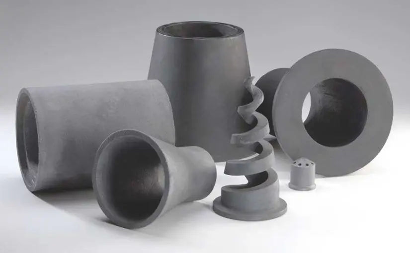
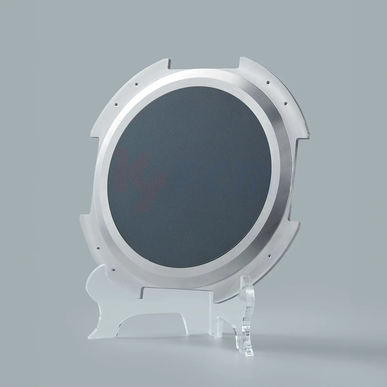
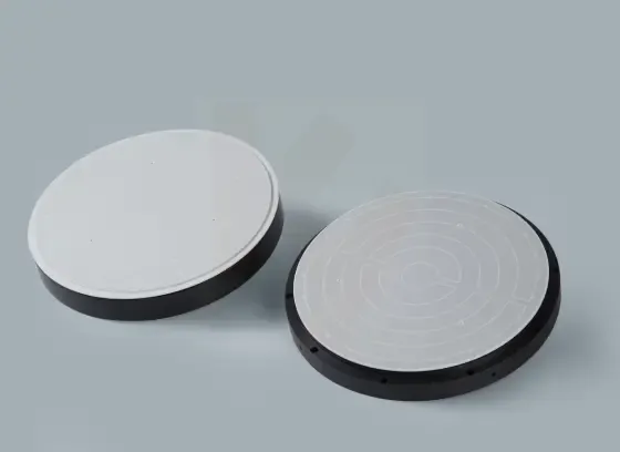 SiC Low-Resistivity Conductive Ceramics for High-Performance Electrostatic Chucks (E-Chucks)
Moreover, SiC ceramics maintain structural integrity at temperatures exceeding 1400°C, with excellent thermal shock resistance. This makes them perfectly suited for processes involving rapid heating and cooling, such as rapid thermal processing (RTP) or atomic layer deposition (ALD), where thermal stress can crack conventional materials. The combination of high thermal conductivity and low thermal expansion ensures uniform temperature distribution across the chuck surface, minimizing wafer warpage and improving process control.
Precision Control Through Ultra-Low Resistivity
The key to effective electrostatic clamping is fast, uniform, and controllable charge distribution. Conventional dielectric or semi-conductive ceramics often suffer from slow response times and uneven potential fields. In contrast, ultra-low resistivity SiC ceramics enable rapid charging and discharging, allowing for millisecond-level adsorption and release of 300mm and future 450mm wafers. This responsiveness enhances throughput and reduces risk during delicate handling operations.
Thanks to precise doping and advanced sintering techniques, the electrical properties of SiC conductive ceramics can be finely tuned. This allows manufacturers to design multi-zone electrodes with tailored resistivity profiles, enabling zonal temperature control and adaptive clamping force distribution—critical for managing edge effects and stress gradients on large-diameter wafers.
Mechanical Durability Meets Cleanliness
With a Vickers hardness exceeding 20 GPa and flexural strength above 300 MPa, SiC conductive ceramics outperform traditional materials in wear resistance and mechanical robustness. They withstand repeated robotic loading/unloading without chipping or surface degradation, eliminating a major source of particle contamination. Their non-magnetic and electrically stable nature also ensures compatibility with sensitive metrology and inspection tools.
Unlike metal components, SiC ceramics do not require plating or coating, removing the risk of delamination. Their intrinsic homogeneity ensures consistent performance over time, batch after batch.
Applications Beyond Standard E-Chucks
Beyond standard Coulombic or Johnsen-Rahbek-type chucks, SiC conductive ceramics open doors to innovative designs:
- High-power plasma etch reactors
- EUV lithography systems requiring ultra-clean, non-outgassing materials
- High-temperature CVD and MBE chambers
- Advanced packaging and compound semiconductor processing
As the semiconductor industry pushes toward more complex 3D architectures and heterogeneous integration, the need for intelligent, durable, and contamination-free wafer handling will only grow. SiC low-resistivity conductive ceramics represent a foundational advancement in E-chuck technology—delivering unmatched performance, longevity, and process stability.
For semiconductor equipment manufacturers seeking to enhance system uptime, improve yield, and meet the demands of next-gen fabrication, the choice is clear: upgrade to SiC-based electrostatic chucks and power the future of chipmaking.