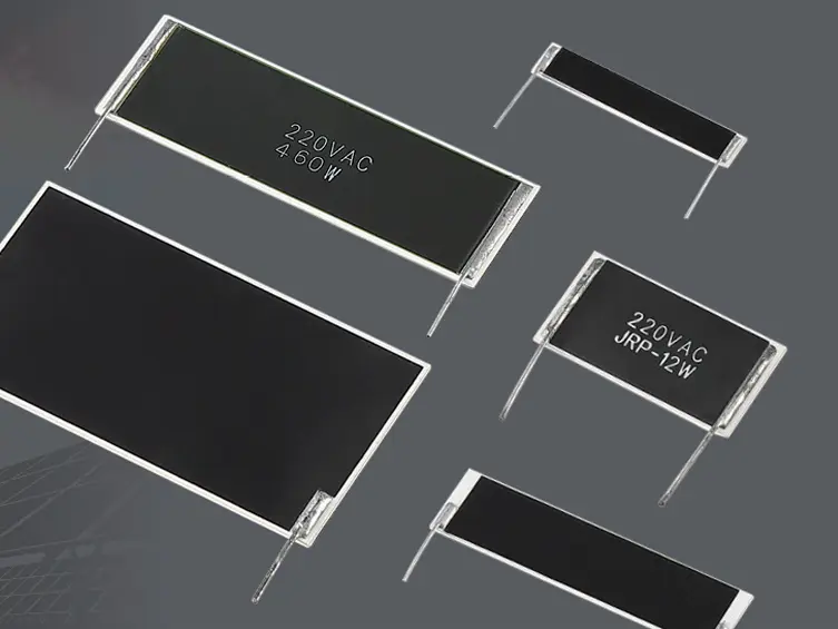
When people hear “high-voltage resistor” they usually picture a bulky ceramic rod. Yet modern voltage-sensing circuits inside 36 kV GIS, EVT or X-ray power supplies are increasingly dominated by a flat, low-profile component that measures barely 50 mm × 12 mm but still holds off 50 kV DC: the thick-film chip high-voltage resistor. Below we unpack how this alumina flake is made, why it outperforms wire-wound blocks, and what engineers should know before specifying it.
1. From ink to kV
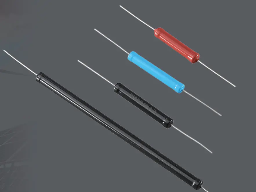
The manufacturing process starts with a 0.6 mm substrate of 96 % Al₂O₃. A screen-printed paste containing ruthenium oxide and glass powder is laid down in a meander pattern, fired at 850 °C, and laser-trimmed to the target value. Because the track is only 25 µm thick and planar, parasitic inductance stays below 80 nH—an order of magnitude lower than a spiral wire-wound part. Multiple layers can be stacked, so a single chip achieves 200 Ω – 1 GΩ while withstanding continuous fields of 700 V mm⁻¹.
2. Electrical highlights
Voltage range: 3 kV – 50 kV DC in one chip
Tolerance: ±0.1 % to ±10 % (laser cut)
TCR: ±25 ppm K⁻¹ typical (25 °C – 105 °C)
Power: 0.5 W – 5 W at 40 °C substrate temperature
Lightning impulse: 70 kV (1.2/50 µs) five pulses pass
Insulation: 12 kV AC between terminations and heatsink
3. Thermal reality
Heat leaves the chip axially through copper or Kovar end-tabs and radially through the silicone coating. Keeping the alumina centre below 155 °C guarantees <0.4 % drift after 1 000 h. Because the coating has an emissivity of 0.9, a simple aluminium clamp on each end can double the usable wattage without forced air.
4. Why “chip” matters
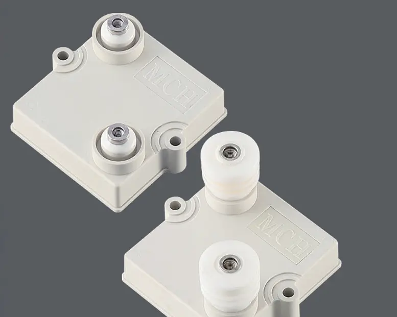
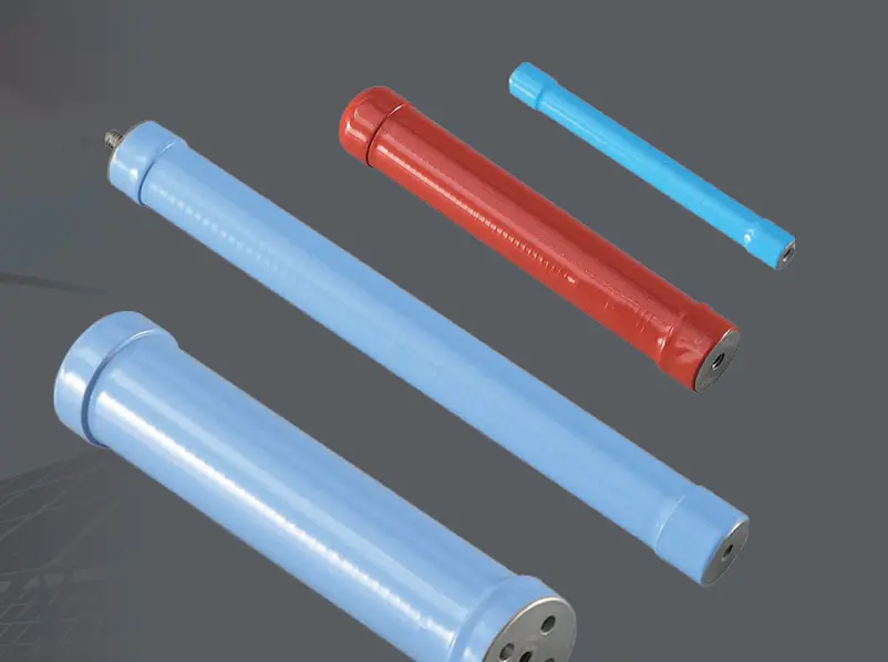
Flat construction means the resistor can lie against a PCB, bus-bar or cast-resin wall, shaving millimetres off GIS phase spacing and allowing automated pick-and-place instead of hand wiring. For pulse applications, the low inductance eliminates overshoot that would otherwise require extra snubbers.
5. Applications you’ll recognise
Electronic voltage transformers (EVT) 10 kV – 36 kV
GIS internal voltage sensors (50 Hz & 60 Hz)
X-ray generator tube current control 40 kV – 120 kV
HV DC link divider in solar string inverters 1 500 V
Pulse modulator feedback 20 kV, 1 µs rise-time
6. Design checklist
Choose resistance so divider current is 0.2 – 1 mA; self-heating then <0.25 W.
Leave 20 % impulse margin—50 kV nominal means 60 kV rated part.
Provide 1 kV mm⁻¹ creepage; silicone-coated versions add 30 %.
Use M3/M4 screws at 1 Nm—over-torque cracks alumina.
Derate linearly from 40 °C: –1.2 % per °C above 155 °C substrate.
7. Reliability snapshot
Thermal shock –55 °C ↔ +125 °C 100 cycles ΔR ≤ 0.2 %
56-day moisture 95 % RH ΔR ≤ 0.5 %
5 × rated power 5 s overload ΔR ≤ 0.3 % Field data show <0.1 % drift after five-year 24/7 operation inside 36 kV GIS.
8. Bottom line
If board space, inductance or weight is critical, the thick-film chip high-voltage resistor is no longer a niche—it is the default building block for precision HV sensing. Specify voltage first, power second, and always keep the alumina cool; the kV will look after themselves.